I work on hardware-software co-design at IBM and teach it at Columbia. The phrase still sounds like jargon to most people. It is about to become common sense, and here is why.
For most of computing history, software got faster on its own. You wrote your code, and every couple of years a new chip arrived that ran the exact same code noticeably faster. You did nothing and were rewarded. That was not luck. It was a physical scaling law, and it ended in the mid-2000s.
Two different scaling laws were doing that work, and it is worth keeping them apart.
Moore's Law is the one people remember. It says the number of transistors on a chip roughly doubles every two years. It is about density, and it is still mostly holding, though it has slowed.
Dennard scaling is the one that actually gave you the free speedup, and it is the one that broke. In 1974 Robert Dennard observed that as a transistor gets smaller, its power density stays constant, so each new generation can run at a higher clock frequency inside the same power budget. More transistors, all switching faster, for the same energy. That is why clock speeds climbed from megahertz to gigahertz for three straight decades.
Around 2005, Dennard scaling ended. Transistors kept shrinking, so Moore's Law carried on, but they stopped getting proportionally more efficient. Push the clock higher now and the chip runs too hot to cool. Clock frequency settled near a few gigahertz, and single-thread performance, the thing that made old software faster for free, settled with it.
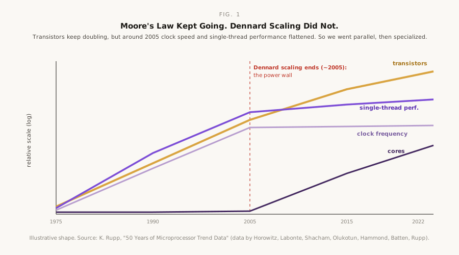 Fig. 1: Transistor counts kept doubling, but around 2005 clock frequency and single-thread performance flattened. The industry responded first with more cores, then with chips built for specific jobs. Illustrative shape; source: Rupp, 50 Years of Microprocessor Trend Data [10].
Moore's Law kept handing us more transistors. Dennard scaling stopped telling us how to turn them into a faster single core. So the industry did the only thing it could. It spent the extra transistors on more cores, and then on chips built for specific jobs.
John Hennessy and David Patterson, who have watched this longer than almost anyone, called what comes next "a new golden age for computer architecture" [1]. Their argument is blunt. If you can no longer make one general-purpose chip faster for everyone, you make specialized chips that are much faster for someone. And the way you do that well is to stop designing the hardware and the software in separate rooms.
That is co-design. It is the strategy that replaced the automatic speedups.
What co-design actually means
For decades the layers of the stack were designed separately. Researchers designed an algorithm and handed it to the software people. The software people wrote a compiler and a runtime and handed it to the hardware people. The hardware people built a chip and handed it back up. Each layer improved itself and assumed the others were fixed.
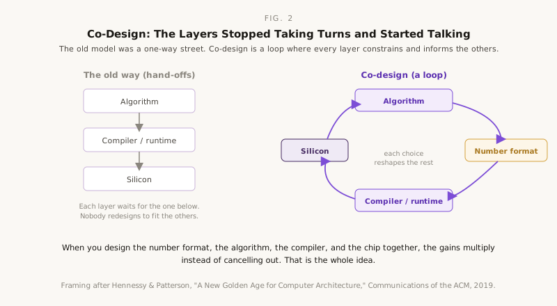 Fig. 2: The old model handed work down a one-way street. Co-design is a loop where the number format, the algorithm, the compiler, and the chip are shaped to fit each other. Framing after Hennessy & Patterson, 2019.
Co-design closes that loop. You choose the number format with the chip in mind. You shape the algorithm around the memory hierarchy. You build the silicon around the operation that dominates the workload. Each decision constrains and informs the others, and the gains compound instead of cancelling out. I made the ground-level version of this case in Why Every AI Engineer Needs to Understand Hardware. This is the same idea one level up, as a design philosophy rather than a personal skill.
The best way to see it is through a few examples where it clearly worked.
Build the chip around the operation
Around 2013, Google did the math on what would happen if every user talked to its speech models for a few minutes a day. The compute bill was frightening. So instead of buying more general-purpose hardware, they built a chip that did almost nothing except the one operation neural networks live on: matrix multiply.
The Tensor Processing Unit is a systolic array, which is a grid of small multiply-add units. The weights stay in place inside the grid, activations enter from one edge, partial sums accumulate as the data passes through, and results come out the other side. There is almost no instruction fetching, no branch prediction, none of the instruction-handling logic a CPU spends most of its energy on. It is arithmetic built directly into the hardware.
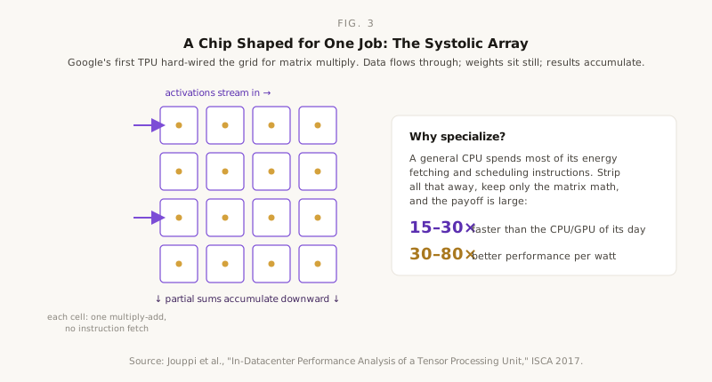 Fig. 3: The systolic array hard-wires the grid for matrix multiply. Data flows through, weights stay put, results accumulate. Source: Jouppi et al., ISCA 2017.
The payoff was not incremental. In Google's own analysis, that first TPU ran its target workloads 15 to 30 times faster than the contemporary CPU or GPU, and delivered 30 to 80 times better performance per watt [2]. You do not get numbers like that from a better algorithm alone, or a better chip alone. You get them from deciding what the chip is for and designing the software to feed it.
Co-design the number itself
Precision is my favorite example, because it shows co-design in miniature. A model does not have to store each number in 32 bits. If it can tolerate less, you can use 16, or 8, or 4, and every halving cuts both the memory you move and the work per multiply.
But you cannot just reduce the bits. Dropping to 8-bit floating point on its own would wreck accuracy, because you lose numeric range. What made it work was three things designed together: the format, a training method that scales each layer to the range it actually needs, and silicon that runs the whole scheme directly. NVIDIA ships this as the Transformer Engine, and it reports that 8-bit floating point halves storage and doubles throughput versus 16-bit while converging about as well [3]. The format, the training method, and the hardware arrived together. Remove any one and it does not work. I traced where this ends up in production in Why Quantization Won.
Let the hardware shape the algorithm
Co-design runs in both directions. Sometimes the chip's constraints change the algorithm.
Structured sparsity is the cleanest case. Roughly half the weights in a trained network can often be removed with little accuracy loss, but a chip cannot easily skip zeros scattered at random positions. So NVIDIA defined a pattern the hardware can use: in every group of four weights, two must be zero. Prune your model to that exact two-in-four pattern and the sparse tensor cores skip the zeros and run the matrix multiply at twice the rate [4]. Notice what happened. The hardware defined a rule, and pruning methods were redesigned to match it. Neither side would have chosen that pattern on its own.
FlashAttention is the same idea applied to memory. The textbook way to compute attention writes a large intermediate matrix out to slow memory and reads it back. Tri Dao and his coauthors rewrote the algorithm to keep the working data in fast on-chip memory and never write that matrix out, which gave a 3 times speedup on GPT-2 and made much longer context lengths practical [5]. The result is identical. The difference is that the algorithm was designed around how the hardware's memory is actually laid out.
The far end: designing for physics
Take co-design far enough and you stop moving data to a processor at all. You do the computation inside the memory.
This is a large part of what my group at IBM Research works on, and it is co-design taken to its limit, because you are mapping the mathematics directly onto the physics of a memory device. Store the weights as conductances in a grid, apply the inputs as voltages, and the currents that emerge are the multiply-accumulate, computed in place by physics. Our 64-core analog in-memory chip reaches about 9.76 trillion operations per second per watt for the matrix-vector math that dominates inference [6]. IBM's NorthPole chip, which keeps all its memory on-chip beside the compute, delivered 25 times more frames per joule than a graphics processor on a comparable process [7].
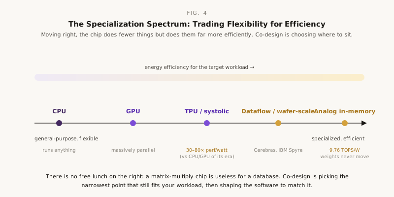 Fig. 4: Moving right, a chip does fewer things but does them far more efficiently. Co-design is choosing the narrowest point that still fits your workload, then shaping the software to match. Sources: Jouppi et al. 2017; IBM, Nature Electronics 2023 and Science 2023.
Between the general-purpose GPU and the analog extreme sits a whole spectrum. Wafer-scale engines from Cerebras keep an entire model's memory on one piece of silicon, right next to the compute [8]. IBM's Spyre accelerator maps the dataflow graph spatially onto reconfigurable cores rather than time-slicing one fixed pipeline [9]. Every one of these is a different answer to the same question: given this workload, how much generality can I give up in exchange for efficiency?
My take, from the systems side
There is a real cost to the specialized end. A matrix-multiply chip is useless for a database, and an analog array that is very efficient at inference is not where you train your next model. Co-design is not about chasing the most exotic hardware. It is about matching your workload to the right chip, and then being willing to redesign the software to fit it. The teams that do this well are the ones where an algorithms person, a compiler person, and a hardware person work together and disagree productively. That collaboration is where the gains come from now.
The skill the next decade rewards
The automatic speedups are not coming back. General-purpose chips are not going to start making everyone's code faster again, because the physics that used to do that stopped in the mid-2000s. What we have instead is a growing set of specialized machines and a growing need for software that knows how to use them.
That changes what it means to be good at this. The valuable skill is no longer deep knowledge of one layer. It is the ability to reason across all of them, to see that a change in the number format leads to a change in the training method leads to a change in the chip you should buy. Most curricula still teach the layers one at a time, in separate courses, as if the old separation still held. It does not. The people who learn to reason across the whole stack, and there are not enough of them yet, are going to design the systems everyone else runs on.
References
[1] John L. Hennessy, David A. Patterson, "A New Golden Age for Computer Architecture," Communications of the ACM, vol. 62, no. 2, February 2019 (Turing Lecture).
[2] Norman P. Jouppi et al., "In-Datacenter Performance Analysis of a Tensor Processing Unit," ISCA 2017. On average 15 to 30 times faster than the contemporary CPU/GPU, with 30 to 80 times better performance per watt.
[3] NVIDIA, "NVIDIA Hopper Architecture In-Depth," 2022, and "Floating-Point 8: An Introduction to Efficient, Lower-Precision AI Training," 2025.
[4] NVIDIA, "Exploiting NVIDIA Ampere Structured Sparsity with cuSPARSELt," 2020. 2:4 fine-grained structured sparsity doubles sparse tensor-core throughput.
[5] Tri Dao, Daniel Y. Fu, Stefano Ermon, Atri Rudra, Christopher Ré, "FlashAttention: Fast and Memory-Efficient Exact Attention with IO-Awareness," NeurIPS 2022.
[6] Manuel Le Gallo, Riduan Khaddam-Aljameh, et al., "A 64-core mixed-signal in-memory compute chip based on phase-change memory for deep neural network inference," Nature Electronics, vol. 6, 2023.
[7] Dharmendra S. Modha, et al., "Neural inference at the frontier of energy, space, and time," Science, vol. 382, October 2023.
[8] Cerebras Systems, "Cerebras Unveils World's Fastest AI Chip with 4 Trillion Transistors" (Wafer-Scale Engine 3), 2024.
[9] IBM Research, "Introducing the IBM Spyre AI accelerator chip," 2024.
[10] Karl Rupp, "50 Years of Microprocessor Trend Data," based on data by M. Horowitz, F. Labonte, O. Shacham, K. Olukotun, L. Hammond, C. Batten, and K. Rupp (CC BY 4.0).
Discussion
Sign in with GitHub to leave a comment or react. Threads are public and live in this site's GitHub Discussions.